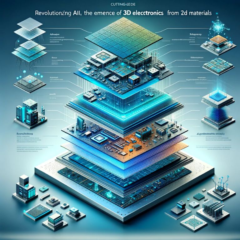
In the rapidly evolving landscape of artificial intelligence (AI) and electronics, the integration of 3D electronics using 2D materials represents a groundbreaking development. This fusion is not just an incremental step forward but a transformative approach that reshapes how we think about and engineer AI hardware.
The Concept Explained
At its core, the idea revolves around leveraging the unique properties of two-dimensional (2D) materials to develop three-dimensional (3D) electronic structures. Unlike traditional 3D electronics, which are typically built layer by layer in a planar fashion, this new approach involves stacking ultra-thin layers of 2D materials vertically. This method allows for more compact, efficient, and powerful electronic systems.
Historical Context and Evolution
The journey towards integrating 2D materials into 3D electronics stems from the limitations of conventional semiconductor technologies. As the demand for more powerful, energy-efficient, and smaller electronic devices has grown, the need for innovation in material science has become paramount.
The Emergence of 2D Materials
2D materials, first brought into the limelight by the discovery of graphene, have emerged as potential game-changers. These materials are just one or a few atoms thick, offering exceptional electrical, thermal, and mechanical properties. Their ultra-thin nature allows for high electron mobility, making them ideal for high-speed and miniaturized electronic components.
The Shift to 3D Electronics
The shift from 2D planar to 3D stacked electronics represents a significant leap. In traditional electronics, as components are miniaturized, issues like heat dissipation and electron leakage become more pronounced, limiting performance. 3D electronics, however, use space more efficiently, enabling higher component densities without these downsides. By stacking 2D materials, it’s possible to create more complex, multifunctional structures in a smaller footprint, offering a new dimension to AI hardware design.
The Impact
The impact of this technological evolution is profound. It opens the door to creating AI systems that are not only more powerful but also more energy-efficient and compact. This advancement is particularly crucial in the era of Big Data and the Internet of Things (IoT), where vast amounts of data need to be processed quickly and efficiently.
Understanding 2D Materials: Properties and Potentials

The advancement of 3D electronics using 2D materials is rooted in the unique and compelling properties of these materials. To fully appreciate this technological leap, it’s essential to understand what 2D materials are, their characteristics, and why they stand out from traditional materials used in electronics.
Characteristics of 2D Materials
2D materials are defined by their extremely thin structure, often only a few atoms thick. This gives them a set of remarkable properties:
- High Electrical Conductivity: Many 2D materials exhibit excellent electrical conductivity. Electrons in these materials face minimal scattering, allowing for faster electron transport compared to bulk materials.
- Strength and Flexibility: Despite their thinness, 2D materials are incredibly strong. They can also be flexible, which opens up new possibilities for flexible electronic devices.
- Large Surface Area: The surface-to-volume ratio in 2D materials is exceptionally high. This aspect is crucial for applications like sensors, where surface interactions play a significant role.
- Optical Properties: Some 2D materials are transparent yet conductive, a rare combination in materials science, making them suitable for applications in transparent electronics and photovoltaics.
- Thermal Conductivity: These materials can also have high thermal conductivity, which is vital for dissipating heat in electronic devices.
The Potentials of 2D Materials in Electronics
The potentials of 2D materials in revolutionizing electronics, especially in AI hardware, are vast:
- Miniaturization: Their thin nature allows for the development of ultra-compact devices, crucial for the miniaturization trend in electronics.
- Performance Enhancement: The high electron mobility in 2D materials leads to faster processing speeds, a key factor for AI and high-performance computing.
- Energy Efficiency: 2D materials can operate with less power, reducing the energy footprint of devices – a crucial factor in sustainable technology development.
- Innovative Applications: From flexible displays to ultra-sensitive sensors, the unique properties of 2D materials enable applications that were previously unfeasible.
The Leap to 3D: Integrating 2D Materials in AI Hardware
The integration of 2D materials into three-dimensional (3D) electronic structures marks a significant advance in artificial intelligence (AI) hardware. This transformative approach, known as monolithic 3D integration, layers ultra-thin 2D materials vertically, creating compact, efficient, and powerful electronic systems.
Process of Monolithic 3D Integration
In monolithic 3D integration, the process begins with layering, where different 2D materials, each possessing unique electronic properties, are stacked vertically. This is followed by establishing vertical electrical connections, or vias, between these layers to facilitate efficient signal transmission across the 3D structure. The final step is the integration of these layers into a cohesive unit, ensuring the structure functions as a unified, efficient electronic system.
Benefits for AI Computing
The shift to 3D electronics using 2D materials brings several key benefits to AI computing. Enhanced processing power is achieved as the proximity of components in a 3D structure reduces signal travel time, crucial for faster data processing in AI tasks. This architecture also allows for a higher component density, enabling more complex AI algorithms to be executed on smaller devices. Energy efficiency is another significant advantage, as the 3D integration reduces power consumption, aligning with sustainable development goals in AI hardware. Additionally, the combination of 2D materials and 3D design improves heat management, crucial for maintaining high performance without the risk of overheating.
Illustrative Table: Comparing 2D and 3D Integration
In contrasting traditional 2D integration with 3D integration using 2D materials, the differences are stark. While 2D integration lays out components horizontally, 3D integration stacks them vertically, enhancing processing speed and component density. The vertical stacking in 3D integration offers improved energy efficiency and heat management compared to the standard levels in 2D integration.
Technological Innovations: 3D Hetero-Integration Technology

The emergence of 3D hetero-integration technology is a pivotal innovation in the field of electronics, particularly in the realm of AI hardware. This technology leverages the unique capabilities of 2D materials to create novel 3D circuitry, offering transformative potential in electronic device fabrication and functionality.
Explaining 3D Hetero-Integration
3D hetero-integration refers to the process of vertically integrating dissimilar materials and components to form a cohesive 3D electronic system. Unlike conventional methods that rely on homogeneous material structures, hetero-integration combines various 2D materials, each with distinct properties, to achieve specific functionalities within a single device. This approach allows for the creation of complex electronic systems that are more than the sum of their parts.
Key Steps in 3D Hetero-Integration:
- Material Selection: Careful selection of different 2D materials based on their electrical, optical, and mechanical properties.
- Layer Stacking: Precise stacking of these materials in a vertical arrangement to form a multi-layered structure.
- Inter-layer Connectivity: Establishing efficient electrical connections between layers, ensuring seamless signal transmission.
- Functional Integration: Combining various functionalities, like sensing, processing, and memory, into a single compact unit.
Impact on Electronics and Circuitry
The impact of 3D hetero-integration on electronics is profound:
- Enhanced Functionality: By combining different materials, the technology enables the creation of electronic devices with enhanced and multiple functionalities in a single compact structure.
- Improved Performance: The vertical integration leads to shorter interconnect distances, reducing latency and power consumption, which is critical for high-speed electronic devices.
- Design Flexibility: This approach offers unparalleled design flexibility, allowing for the customization of electronic devices for specific applications.
- Scalability and Compactness: 3D hetero-integration enables the construction of more complex systems in a smaller footprint, vital for the miniaturization trend in electronics.
Multifunctional Chips and AI Advancements
The advancement of 3D electronics from 2D materials has given rise to multifunctional chips, which are revolutionizing the capabilities and applications of artificial intelligence (AI) hardware. These chips integrate various components—sensors, processors, and memory—into a single unit, significantly enhancing the functionality and efficiency of AI technologies.
Role of Integrated Sensors, Processors, and Memory
In these multifunctional chips, integrated sensors play a pivotal role in detecting a wide array of environmental parameters, providing essential data for AI systems. The processors within these chips are tasked with executing complex AI algorithms at high speeds, making them the core of AI computations. Alongside these, memory units embedded in the chips store data and instructions, facilitating swift execution of AI tasks and reducing the dependence on external memory sources. The convergence of these components in a single chip results in a compact, efficient, and versatile unit capable of performing various functions simultaneously.
Enhancing Computer Chip Functionality
The utilization of 2D materials in the fabrication of these chips significantly elevates their functionality. These materials contribute to improved speed and efficiency in data processing while ensuring reduced energy consumption. The structural stability and strength of 2D materials enhance the durability and reliability of the chips, crucial for long-term and demanding AI applications. Furthermore, the versatility of 2D materials allows for flexible design customization, catering to specific AI tasks. In terms of sensing capabilities, the heightened sensitivity of 2D materials amplifies the performance of integrated sensors, yielding more responsive and accurate results.
Impact on AI Computing
The emergence of these multifunctional chips has a profound and far-reaching impact on AI computing. They facilitate the miniaturization of AI systems, making them suitable for applications where space and power are constrained. These chips significantly expand the capabilities of AI systems, enabling them to perform more complex operations. Moreover, their energy-efficient nature aligns with the growing need for sustainable AI solutions.
Future Prospects and Challenges
As the field of 3D electronics from 2D materials continues to evolve, it presents a blend of exciting prospects and formidable challenges that will shape the future of AI and electronics.
Potential for AI and Electronics
The integration of these advanced materials is set to revolutionize AI computing by facilitating the development of more sophisticated AI applications capable of real-time processing and decision-making. This technology is also expected to spur the creation of innovative electronic devices, ranging from wearable technology to advanced IoT devices. Furthermore, the energy efficiency of 2D materials is particularly promising for sustainable technology development, offering greener alternatives in electronic device manufacturing. Another significant prospect is the potential for greater integration and miniaturization of electronic components, which could open new avenues in diverse sectors such as healthcare, automotive, and consumer electronics.
Challenges Ahead
However, this technological advancement is not without its challenges. One of the primary hurdles is the development of efficient and scalable methods for synthesizing 2D materials, which is critical for the broader adoption of this technology. Additionally, the complexity involved in integrating different 2D materials into a unified 3D structure poses significant engineering and fabrication challenges. Ensuring the reliability and consistency of these materials across various environmental conditions is another crucial aspect that requires attention. Moreover, the cost and complexity of manufacturing processes are key factors that need to be optimized to make this technology commercially viable.
Material-Level Solutions and Future Directions
In response to these challenges, researchers are actively exploring material-level solutions and innovative manufacturing techniques. Efforts are underway to develop more cost-effective, scalable methods for producing 2D materials and to refine integration techniques to enhance the reliability and consistency of 3D electronics. As such, while the path forward includes obstacles, the continuous advancements in research and development are paving the way for these revolutionary materials to transition from promising concepts to practical, widespread applications in AI and electronics. The future, therefore, holds immense potential for groundbreaking developments that will redefine AI hardware and the broader landscape of electronic devices.
Conclusion
The integration of 3D electronics from 2D materials represents a paradigm shift in AI hardware and electronic device development. This innovative approach promises more advanced, energy-efficient, and miniaturized AI systems, with applications spanning across various sectors. While the potential of this technology is immense, it also faces challenges in material synthesis, integration, and manufacturing. As research continues to address these challenges, 3D electronics from 2D materials are poised to redefine the landscape of technological innovation. Looking forward, this breakthrough stands as a cornerstone in shaping the future of AI and electronics, heralding a new era of efficiency and capability in the technological world.